CONSTRUCTION of the RX19
********
LIST OF COMPONENTS
Active
IC1 MC3362P
IC2 MC145170P
IC3 MC68HC711D3FN (to be programmed by the author)
IC4 NM93C0N
IC5 MC34064P
T1 J310 TO92
T2 BC859C SMD
T3 BC859C SMD
Resistors SMD (1206 unless indicated)
Capacitors
R1 1 kohms
C1 15 pF* NPO 805
R2 100 ohms
C2 100 pF 805
R3 12 kohms
C3 12 pF* NPO 805
R4 12 kohms
C4 0.1 µF mc/2.5
R5 150 kohms
C5 100 pF NPO 805
R6 12 kohms
C6 22 pF NPO 805
R7 1 kohms
C7 0.1 µF 1206
R8 1 kohms
C8 0.1 µF 1206
R9 3.3 kohms
C9 0.1 µF 1206
R10 100 kohms
C10
220 pF NPO 1206
R11 39 kohms
C11 0.1 µF mc/2.5
R12 3.3 kohms
C12 22 nF 805
R13 10 Mohms
C13 0.1 µF 1206
R14 2.2 kohms
C14 47 pF* NPO 805
R15 120 kohms**
C15 0.1 µF
mc/2.5
R16 2.7 kohms
C16 47 pF 1206
R17 33 kohms
C17 1 µF pt/35V
R18 à R26 390 ohms / 805
C18 22 µF pt/10V
R27 12 kohms/ 805
C19 220 pF 1206
R28 10 Mohms
C20 10
µF pt/10V
R29, R30 33 kohms/ 805
C21 27 pF NPO 805
R31 12 kohms/ 805
C22 27 pF NPO 805
R32 à R34 33 kohms/ 805
C23 0.1 µF 1206
R35 56 kohms/ 805
C24 0.1 µF 1206
R36 47 kohms/ 805
C25 0.1 µF 1206
R37 et R38 56 kohms/ 805
C26 22 ou 33 µF CMS/10V
Caj 22
pF pas de 5
* Pour le 41 MHz : C1=18 pF C3=18 pF C14=68 pF
* For the 41 MHz: C1=18 pF C3=18 pF C14=68 pF
** adjust according to the need of the AGC
805=item size 1206=item size
Others
1 set of special coils L1, L2, L3 and L4 (author)
1 set of printed circuit boards (possibility to group orders)
1 case + decorative decal
1 quartz 10.7 filter MHz, kind like XF106 (Lextronic)
1 ceramic filter CFW455G (Lextronic)
1 quartz 10 MHz in a case HC49/S (from Radio Spares)
1 quartz 10245 kHz, type RX16 (MATEL)
1 PLCC socket SMD 44 pins (RS)
1 block of 4 dip switches ITT CDB4LS (RS)
1 female connector 2.54, 5 pins (RS)
1 32-pin connectors 2.54 (RS)
5 screws of 1.6x10mm, milled head
1 brass nut 1.6mm
Flexible wire for interconnections and antenna
NB. Contact us for any problem of supplies.
Possible bulked orders of parts
2. PREPARATION
Assemble all components, the printed circuit boards, and the case. Proceed to the
cutting of the holes for the connectors.
Best is to use the decoder plate as a gauge. The female connector Conn1 must be embedded
in its cutout space.
The grooves cut in the PCB must be tight fitting, for a good stability of the synthesis.
Tap the five holes to a diameter of 1.6mm.
For the HF module, add a nut welded to the back: screw the nut on a screw of 1.6mm, screw
this screw in the plate,
bring the nut in contact with copper and solder it in place.
Soldering will be much easier if you sand the brass nut before. Remove the screw.
Do not install nuts on the corners of the decoder, but spacers of 6 mm out of brass,
aluminum, or plastic.
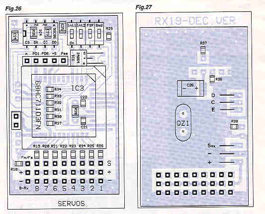
3. INSTALLATION OF COMPONENTS
a) HF Part.
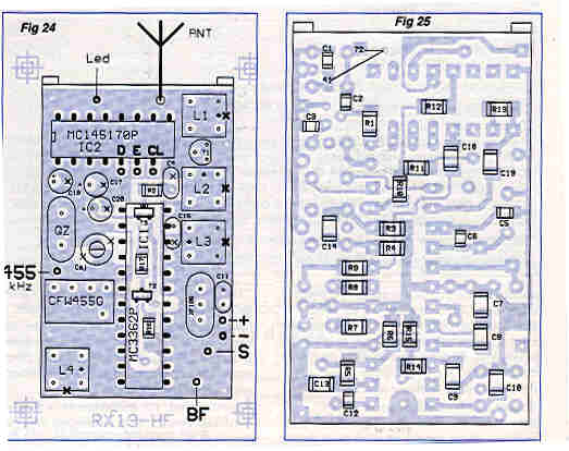
If the holes are not metallized,
install some jumpers front-to-back: under the MC3362 and the 145170. Solder T2, T3, R16
and R17 then R2, C4 and C15. Be careful, the installation of C15 is rather critical. You
will need a thin capacitor.The ground wire does not penetrate through the plate. Fold to
90° and solder it flat on the negative trace.
Take care not to touch pin 22 of the MC3362 and not to block the installation of the
shielding of L3.
You will place these components, temporarily, to check that all is well.
Finish installing the components on the topside and the rotor of Caj next to pin #3. Do
not apply excess solder on the back where SMD components will also be placed. Pin #16 of
the 3362 must be soldered to the negative trace if the holes are not metallized. Do not to
forget the test points, made from simple component leads. Sand the back. Clean with
acetone.
Solder all the components belonging on the back.
N.B. 1 we recommend the systematic measurement of the value of SMD
capacitors. They are not marked and a mistake is, afterwards, very difficult to detect.
N.B. 2 resistors R15 of the RX19 regulates the effectiveness of the
AGC. We can accept an initial value of 120 kOhms, with the recommended transistors.
Nevertheless, we would be able to adjust this resistance according to the following
criteria:
- Without a signal, R2 must deliver the maximum voltage towards T1. If the tension is
already lower, resistance is too large.
- Transmitter switched on with a 12 V light bulb in lieu of the antenna and a few meters
away from the circuit, the AGC must enter in action, lowering the output voltage from R2.
If the tension does not drop on a strong signal, resistance is too low.
b) Decoder
Last version of RX19 is RX19B with a modified decoder :
>>>> RX19B
 If the holes are
not metallized,
If the holes are
not metallized,
work is more delicate because it is necessary to install front-to-back jumpers on the
connectors Conn1, Conn2, and Conn3. Do that with
very fine wire soldered flat, on the topside, extending across the holes
at the same time as the pins. Install
a jumper also under the µC and another along the right edge. At the points of connection
of the servo wires, the male pins should go across the holes completely so to solder them
on both sides. Solder all SMD components
of the topside as well as QZ1. Then solder the PLCC socket, after having removed the
central part. Take care to orient it correctly. Put the pins in the correct place on the
circuit, and then fix the socket with 2 tacks of solder in diagonal.
Make a last check and it is all go
for the soldering of all the other pins. It is easy to guess that an iron with a very fine
tip and 5/10 solder are advised for this work. Once the solderings are made, check the
quality of work with a magnifying glass, then with the ohmmeter.
Finish the installation of the components of the topside. For IC4 and the switches do
not cut the pins that protrude.
They will be soldered front and back. Cut the others as flush as you can. They do not
protrude and should be soldered
on the front only.
4. STARTUP
a) Decoder
Check all work meticulously.
Put the DIP switches to OFF. Insert the µC in its socket. Prepare the powering on of
the decoder alone: battery connected through a switch on OFF. The 93C06 being blank, it
should be programmed to obtain the starting of the normal program.
For that, connect the point Pss of Conn1 to the negative trace and connect a voltmeter
between the point PD1 and the negative. Put the decoder under tension and note the change
of PD1 to 1 or +5 V. It is done, the 93C06 contains the data.
Put the switch to OFF. Remove the ground connection of Pss and remove the voltmeter.
Connect the oscilloscope on a
servo channel output and put under tension. Observe a 1.5 ms ridge on outputs 1 to 7 and
of 1 ms on output 8.
It is good, the decoder works. If you are curious, you can also check the existence of the
signal on Data, Clock and Enable.
b) Receiver
Connect the two PCB’s using two cords of three twisted wire of 5-cm length
approximately.
We always bring the HF module in service cups in place, not glued, without the shielding.
Screw L1, L2, L3 and L4 coils’ cores in a little but not completely, using the
appropriate tool.
Power up, put the oscilloscope between "Led" (fig. 24) and the negative trace.
Adjust L3 to have a base line at the high level, with very fine negative impulses, to 5
kHz.
If that does not work, check:
- The arrival of Date, Clock and Enable signals;
- The possibility to adjust VCO by L3 on the frequency necessary, i.e. 61550 kHz in 72 and
30400 kHz in 41 MHz;
- The existence of 10245 kHz on pin#2 of 3362 initially and on 145170 after;
- The integrity of the input connection of 145170 (R9, C16) and of output (R10 with R12,
C15 and C17).
All that to prevent the worse which only happens if you have badly worked!
The synthesis functioning, connect the oscilloscope between "BF" (fig. 24) and
the negative trace where one must
observe the usual curve to be set to the maximum through L4.
Put the SUPERTEF under tension, programmed on Fn = Fs = 72250 or 41100 kHz and a code
of "86".
Replace the antenna with a 12V/0.1A light bulb. The signal should appear. Adjust to the
highest value using L4 to about
800 mVcc. The future connected servos must answer (simply check the signals with the
oscilloscope).
If the adjustment of the transmitter’s frequency is correct, measure the 455 kHz at
the point "455" (fig. 24).
Adjust FI2 to this value using Caj. Re-adjust L4. Lastly, move the transmitter away until
having a rather strong curve on
the oscilloscope. Adjust L1 and L2 to reduce this curve as much as possible.
Determine if necessary the right value of R15. See Note#2.
5. LAST ADJUSTMENTS
See
also HOW TO ADJUST THE RECEIVERS.
Glue the cups with araldite. Place the shieldings one leg removed and solder the other.
Install the PCB’s in their casing.
Place a thin and hard insulator between the bottom and the HF part.
Re-do all the adjustments of the RX19, like above.
For L3, we program the SUPERTEF on the two limiting frequencies of the band and we adjust
this coil to have the same quality of impulse as measured on "Led" with the two
frequencies.
The balancing of L1 and L2 is done on the middle frequency of the band.
Fine tune the 455 kHz using Caj and finish by the final adjustment of L4. Glue the cores
permanently with wax.
6. USE
a) Initial programming.
To be done at the first startup or re-do if necessary:
- Temporarily connect Pss (PC7) to the negative trace
- Switch on the RX19
- The line PD1 indicates 1 when the programming of 93C06 is complete
- Turn the RX19 OFF and ON again. It uses the following data:
Fn = Fs = 72250 or 41100 kHz
PPCM code = 86
Channels 1 to 7 = 1.5 ms
Channel 8 = 1 ms
Average impulse = 450 µs
b) Programming RX19 by SUPERTEF
This can be done using a direct cable or an IR system.
IMPORTANT: press on the button BEFORE the powering up of the RX19. Keep pressing while
powering up.
Line PD1 indicates 1: The RX19 awaits data.
Send the data while following the instructions of the screen of the SUPERTEF. Line PD1
returns to 0. Disconnect.
Switch off the RX19.
Switch the RX19 on again for it to use the new values of Fn, Fs and Code
c) Programming of the average impulse
This adjustment makes it possible to optimize the sorting of short and long impulses of
code PPCM.
Place DIP switch1 (PC6) and DIP switch2 (PC5) in ON position.
SUPERTEF must emit a signal whose code contains, in binary, FOUR " 0 " and FOUR
" 1 ", for example " 86 " which is written as " 01010110 "
or " 170 " which is written as " 10101010 ". The RX19 is programmed on
this code and it receives indeed the signal which activates the servos. The RX19 must NOT
be on FAIL SAFE! Temporarily connect PC7 to the negative trace, with a push rod on Conn1
between Pss and the trace. Line PD1 indicates 1. It is done.
Switch the RX19 OFF and ON again.
d) Programming CONTROGAZ
Only turn DIP switch2 (PC5) to ON.
Proceed as in c) above except by positioning channel 7 (CONTROGAZ channel) on the desired
position.
Of course, to use the mode CONTROGAZ, channel 7 of transmitter must have for origin the
stick controlling gas,
therefore have an ORIGIN equal to 4 and the gas servo must be connected on channel 7 of
RX19.
e) Programming PROGRAM mode
Only turn DIP switch1 (PC6) to ON. Proceed as indicated in c) above but this time place
ALL the sticks in the position
you choose for the fail safe.
f) Configuration in flight
- Fail Safe
| DIP switch 1 (PC6 ) |
DIP switch 2 ( PC5 ) |
Fail Safe Result |
OFF |
OFF |
Nothing happens |
OFF |
ON |
CONTROGAZ |
ON |
OFF |
PROGRAM |
ON |
ON |
EXTERNAL |
- Direction of the modulation shift. By DIP switch
4 (PC3)
OFF: "Thobois" shift
ON: shift reversed
- Fail Safe Delay. By DIP switch3 (Pc2)
OFF: approximately 2.5 sec.
ON: approximately 1.25 sec.
- In flight:
Do not press on Pss
Buzzer alarm on PD1 by Conn1